Showing posts with label DistoMatic. Show all posts

Tuesday, April 29, 2014

If 3 is good then 4 is better

The last post about KiCad (here) was based on the DistoMatic series of boards (eventually there'll be several). I'm trying standardize my connections to simplify the process and allow for greater use.

Previously my pinouts were this:
  1. 3v3
  2. 5v
  3. GPIO
  4. Analog
  5. GIO
  6. Ground
This works fine for the Ping))), MaxBotix, SharpIR, etc. sensors, as they only need voltage, ground, and 1 or 2 signal lines.

I came up with this pinout based on the MaxBotix so that one may be able to connect the sensors so that one can trigger the next one. The trigger-out from sensor #1 would go to the trigger-in to sensor #2.

But I was think that many devices use the SPI (wiki definition) protocol and it wouldn't work with my own spec. That needs Clock, Select, DataIn, DataOut pins, 1 more than what I have available. However, if I remove one of the power lines, then I would have 4 lines for data.

So going forward I'm going to only supply 5v to the my boards. If the sensor or breakout board needs only 3v3, then I can use a voltage divider or a regulator to bring down the voltage.

New pinout:
  1. 3v3
  2. GPIO
  3. GPIO
  4. Analog
  5. GIO
  6. Ground
I am trying to learn from those who came before me --
  • Gadgeteer has a 10 pin connector protocol, with 3v3, 5v and GND being standard places
  • MikroElectronics has a connector with standardized pinouts for several protocols
  • Arduino has standardized pinouts on the connectors for the mCu breakouts.


Friday, April 11, 2014

More KiCad learning curves - always double check!

The Good, the meh and the bad.

These boards are for the DistoMatic mainboards to inteface with Parallax Ping )))))) ultrasonic sensors.

tl;dr version:

Good news : Got my KiCad designed DistoMatic boards in the mail. 

Meh news : Throughhole pads are not on both top and bottom as they are in Eagle by default.


Bad news: Either the labels are wrong or my pins are in the wrong order in relation to the Ping )))))))).

The Meh

With Eagle, when you place a throughhole connector, it defaults to puttin the pin pads (where you apply 
solder to) to both top and bottom.  Below is the property for the 3 hole connector - notice there's no selection of which PCB layer put the pads on.


Contrast that property window with the one below, which is for the trace (the path for the current to go through on the board) which is set to be placed on the bottom layer.


Here's the corresponding property window for the "pinhead" in KiCad


Notice there's a layer selection in this window that wasn't there in Eagle. Since I was used to the style, I didn't even think to change the defaulted top layer section.

Even so I should have caught this when submitting the design to OSHPark.com. A great feature of their site is that when you upload a project, it will generate a preview of the various different layers.

Here's a previous version of the board (biggest difference being the SMT connector). You can see the gold pads on both the top (left) and bottom (right) layers.

Before ordering, and waiting 2 long weeks, I should have noticed that pads are only on the top (left) layer.

These are things that are taught by experience. Hopefully this helps others to avoid the same issue.


Tuesday, March 18, 2014

A little toasty

I've got so much to learn about this whole process, so I dove right in! 


Duke Nukem from the GHI forums wanted a Gadgeteer Module to connect multiple MaxBotix ultrasonic distance sensors to a mainboard. After some research and designing I came up with my DistoMatic line. I'll discuss these boards a little later on when I have more to show off.

I found connectors which I liked and that were surface mount, and bought some. Putting the cables together was an adventure for another post. In all my research, I neglected to check if they were compatible with non-leaded solder temperature profiles. 

They were not. 

You can see the discoloration when compared to the raw sockets on the left. Also the right most connector is slightly melted - the walls should be perpendicular.


So more research and testing is needed. Lesson learned is that I have much still to learn! But this all part of the learning process I expected. 

Here's a quick overview of my current process.

1 - Prep

I've only used OSHPark.com for my boards thus far so I can't compare, but I've been rather pleased with the results. They provide 3 boards at $5 sq inch, so quite reasonable for prototyping. The ordering process is very easy, all you do is upload your .brd file, they show a preview of the different layers, and then can order it.

Fresh board from OSHPark.com

2 - Apply solder paste.

I submitted my design to OSHStensils.com and in a few days the post man brought me a 3mm stencil to apply the paste. In each order, they also include a plastic business sized card to spread it. The board is being held in place by their Acrylic Stencil Jig ($6) - figured it was the same thickness of the PCB, so it would be useful.


With paste applied

3 - Place the components

The capacitors were placed with a angled tweezers and the sockets were placed by hand. If some of the paste gets smudged by moving the parts, it's ok, within reason. The board has a layer that prevents the solder from sticking to the purple areas, so it adheres only to the exposed pads.

Notice the paste is still gray and all the pads are fully covered 

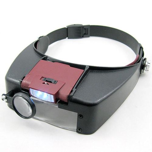
Because the 0603 components are beyond tiny, I got a visor magnifier from ebay for about $8.


4 - Bake 'em

My first attempt for these boards was on #6 (as that worked well on my previous attempts). But the sockets came out brown and slightly misshaped.


Attempt 2 was on profile #3, hoping that the short time at max temp would be ok. Not so much...